Research
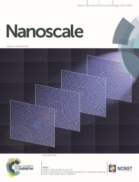
Prof. Zonghoon Lee’s Atomic-Scale Electron Microscopy Lab
Prof. Zonghoon Lee’s Atomic-Scale Electron Microscopy Lab

Abstract
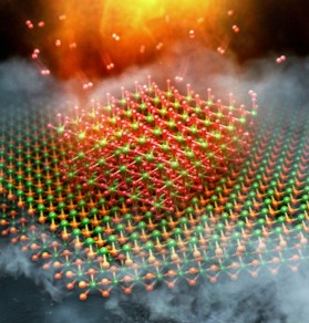
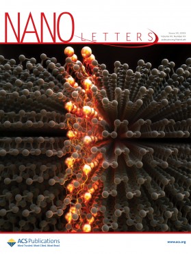
Van der Waals (vdW) epitaxy allows the fabrication of various heterostructures with dramatically released lattice matching conditions. This study demonstrates interface‐driven stacking boundaries in WS2 using epitaxially grown tungsten disulfide (WS2) on wrinkled graphene. Graphene wrinkles function as highly reactive nucleation sites on WS2 epilayers; however, they impede lateral growth and induce additional stress in the epilayer due to anisotropic friction. Moreover, partial dislocation‐driven in‐plane strain facilitates out‐of‐plane buckling with a height of 1 nm to release in‐plane strain. Remarkably, in‐plane strain relaxation at partial dislocations restores the bandgap to that of monolayer WS2 due to reduced interlayer interaction. These findings clarify significant substrate morphology effects even in vdW epitaxy and are potentially useful for various applications involving modifying optical and electronic properties by manipulating extended 1D defects via substrate morphology control.
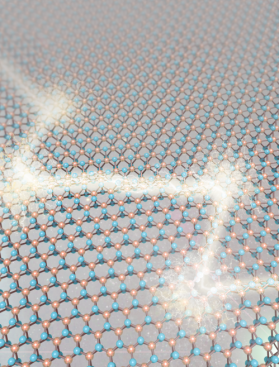
Our research focuses on atomic-scale characterization, design, and synthesis as well as the properties of advanced materials including 2D materials, carbon materials, and soft matter by means of aberration-corrected transmission electron microscopy and spectroscopy. In situ experiments at both the atomic and nano scales are implemented for our study.
Advanced TEM Characterization